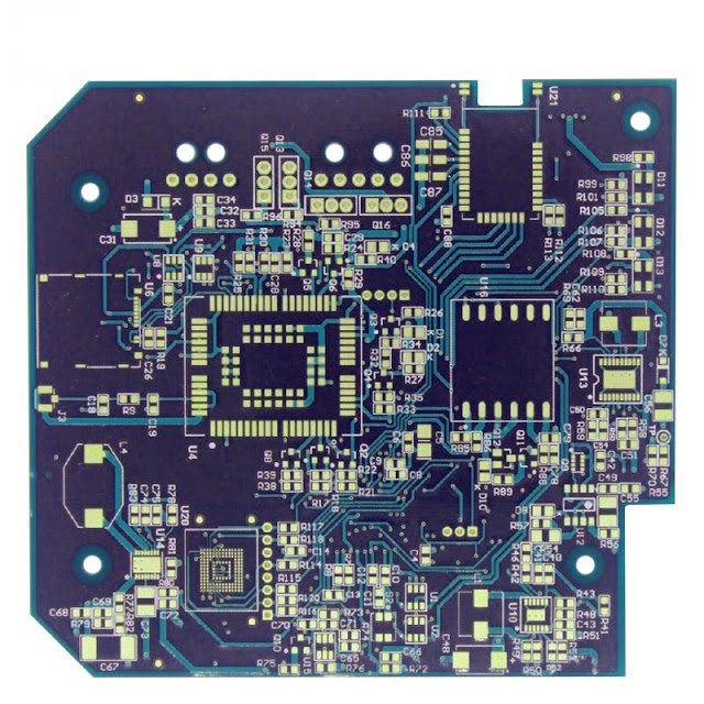
Designing PCBs is an intricate process that requires highly skilled professionals dedicated to excellence in quality. From beginning to end, the process must be precise, detailed, and thoroughly documented to avoid common mistakes. While no one can be perfect, being aware of common mistakes And how to avoid them is the first line of defense against costly rework.
The following list is a simple guide to the most common PCB component mistakes that can occur during design, with tips avoid these common pitfalls.
image source: Alibaba
1. Selecting the Wrong PCB Layout Technique for the Job
There are numerous ways in which to draft the schematic diagram for PCB prototypes—selecting the right layout technique from the start is key. Designers should draft complex designs for use in one or more devices, adding to the importance of precise layout. Some layout techniques are more efficient than others. Consider using an auto-router, which is now a common tool in most computer-aided drafting (CAD) programs, to help maximize the efficiency of the layout.
2. Cutting PCB Design Reviews Short or Eliminating Them to Save Time
Cutting design reviews short or skipping them altogether is never worth it. Design reviews are one of the most vital steps in the overall workflow process. Peer reviews and independent reviews by subject matter experts are the best defense against the most common design mistakes.
3. Selecting the Wrong PCB Design Tool for the Job
Choosing the right tool for the job is one of the most important and fundamental principles in the successful design, development, and manufacture of PCB components. There are many electronic design automation (EDA) CAD software tools available for use today that vary in complexity and ease of use. Compare the features to determine the right design tool for the job at the start. Beginning the design process with wrong or inefficient design tools can create issues such as design delays and increased manufacturing costs down the line.
4. Lack of Effective Team Communication and Collaboration
The most efficient design team is a multi-disciplined team that represents expertise from relevant departments within the business. The design team must work with the software team and housing/enclosure team to ensure all subcomponents of the final product fit and work together. Proper communication methods should be identified in advance and the team held accountable to them throughout the design process.
5. Failure to Back Up the Work
Businesses use different software and varying data sets to achieve the desired outcome during the design process. The speed alone at which data is processed, changed, and stored by high-powered design software can be mind-boggling. Data can be easily lost in an unforeseeable power outage or with the click of the wrong mouse or keyboard button. To avoid this time-consuming mistake, save data often and take care when closing and opening windows and programs on the desktop.
PCBs are an integral part of the electronic products consumers have come to rely upon every day. Avoiding these five common PCB design mistakes will help reduce the chances of costly and ineffective PCB prototypes that can increase the time and expense of getting a final product to market.
Related services:


Comments
Post a Comment